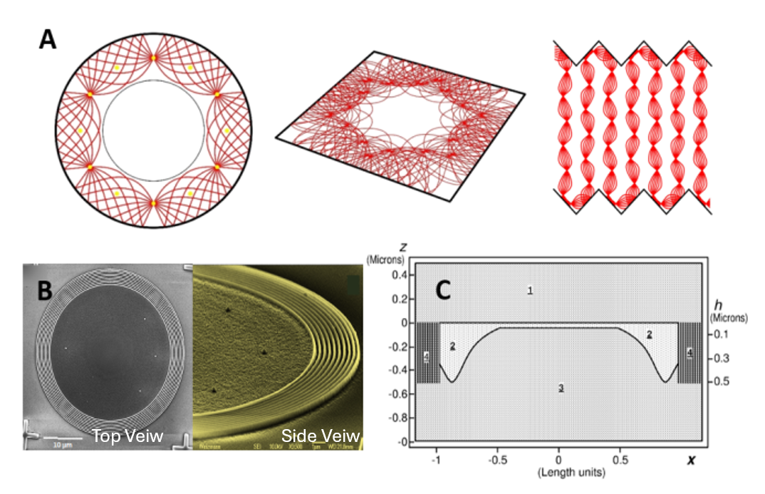
A compact on-chip optical layer that replaces traditional wiring in multi-core processors using silicon photonics. This innovative approach significantly reduces power consumption, heat generation, and space requirements, enabling higher core densities and improved inter-core communication.
- Consumer electronics
- Automotive
- Hardware for deep-learning networks
- Robotics
- Signal processing
- Telecommunication
- Information processing
- Direct and wireless inter-core communication, with scalable connectivity (up to 1000-fold increase)
- Reduced heat output with increased computing power
- Waveguide fabrication is compatible with traditional CMOS fabrication technologies
- Point-to-point communication without crosstalk
Miniature prototypes have been fabricated and successfully tested, demonstrating the feasibility of the technology. In order to achieve the full potential of the technology, prototypes need to be connected externally to many lasers and detectors. A US patent has been granted (10,938,486) and a PCT patent application has been published (WO 2024/176231).

A) Schematic top view of a propagation layer of several geometries of the optical bus. B) SEM images (top and side views) of a prototype manufactured by an e-beam lithography.
C) Schematic cross-sectional view of an optical bus. (1)&(3) - non-propagation layers; (2) - a light propagation layer, (4) - a Bragg mirror (4). The thickness profile of the propagating silicon layer defines the refractive indenx causing light propagation to follow specific propagation paths.


